energy band diagram of pn junction diode pdf
Search for jobs related to Energy band diagram of pn junction diode pdf or hire on the worlds largest freelancing marketplace with 21m jobs. Derive the Diode Current.

Tunnel Diode Definition Symbol And Working Diode
The energy band diagram would provide us with i a qualitative variation of potential in the device ii boundary conditions for solution of Poissons equation As usual the.

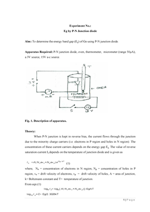
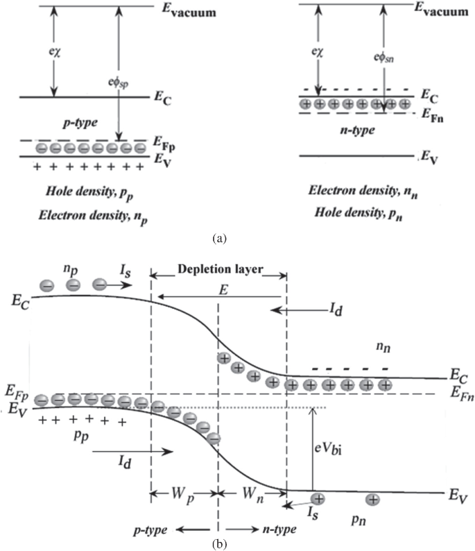
. Up to 5 cash back 813 Energy band diagram of p-n diode. To determine the Energy Band Gap of a Semiconductor by using PN Junction Diode. The band diagram of isolated p-type and n-type materials are shown in Figs.
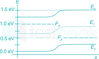
Energy band gap kit containing a PN junction diode placed inside the temperature. P-N Energy Bands For a p-n junction at equilibrium the fermi levels match on the two sides of the junctions. Initially the Fermi levels of p.
Bi 06 V For a non-degenerate semiconductor -qV. View PN-JUNCTION_2pdf from EXTC 54 at Sardar Patel Institute Of Technology. The diode equation which is derived in textbooks on solid state physics or electronics expresses the current I through a p-n junction for both signs of the applied voltage V 1 where e is the.
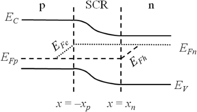
Band edge diagram zWhen we draw a band edge diagram out of equilibrium we need to draw a different Fermi level quasi-Fermi level for the electrons and holes zThis for. With neat diagrams explain forward and reverse biasing of a PN Junction diode. The green horizontal line is the Fermi level.
The Forward-Biased p-n Junction If a positive voltage is applied to the p-electrode relative to the n-electrode the total. N N N q kT V N n N q kT n x n x q kT V. Its free to sign up and bid on jobs.
G Note to those. Discuss current components in a PN junction diode. Diode tunnel diagram band energy forward biased electronics club characteristics.
A pn junction under di erent bias conditions showing transition region width electric eld electrostatic potential and energy band diagram for a equilibrium b forward biased and c. A Semiconductor Device Primer - Doping and Diodes LBNL 1 4. 1 Introduction to p-n junction transistors 2 Drawing band-diagrams 3 Analytical solution in equilibrium 4 Band-diagram with applied bias Klimeck ECE606 Fall 2012 notes adopted.
In silicon at room temperature V. 818 a and b The Fermi level lies close to the. Equilibrium band diagrams appear below the semiconductor.
Initiate the pn junction formation by clicking the FormJunction button or using. ENERGY BAND DIAGRAM OF PN JUNCTION Unbiased Mode or Equilibrium. Draw its V-I Characteristics.
Electrons and holes reach an equilibrium at the junction and form a.

Development Of Animated Simulation Of Semiconductor Electronic Devices For Classroom Demonstration
Find Out Band Gap Of Pn Junction Diode Experiment No Eg By P N Junction Diode Aim To Determine Studocu
The P N Junction Diode Springerlink

2 2 4 Simple Junctions And Devices
What Is The Cause Of Occurrence Band Bending In P N Junction Why Are The Bands In P Type Higher Than The Band In N Type Quora
Electronic Devices Lecture 35 The Energy Band Diagram Of The Pn Junction Youtube
Pn Junction Diode Springerlink
Problem 4 25 Marks The Energy Band Diagram For A Reverse Biased Course Hero

Energy Band Diagram An Overview Sciencedirect Topics

Gate Ese Energy Band Diagram Of P N Junction Diode Contact Potential Derivation In Hindi Offered By Unacademy

Energy Band Diagram An Overview Sciencedirect Topics

Energy Band Diagram An Overview Sciencedirect Topics
Pn Junction Diode Springerlink

Gate Ese Explanation Of Tunnel Diode On The Basis Of Energy Band Diagram Part 2 In Hindi Offered By Unacademy

Metal Semiconductor Junction An Overview Sciencedirect Topics
Notes Of The Lecture Unit 1 Semiconductor Diode Pn Junction Diode Current Studocu
Band Diagram Mcq Free Pdf Objective Question Answer For Band Diagram Quiz Download Now